Objectives and design requirements: The objective is to design and prototype a full-duplex patch antenna system operating in the Very High Frequency (VHF) band, specifically targeting a resonant frequency of 425 MHz. The system employs
one Tx and one Rx element, with an Electromagnetic Band Gap (EBG) structure placed between them to increase isolation between the two antennas. This is critical for mitigating self-interference (SI) and ensuring reliable full-duplex operation.
The antenna should exhibit optimal impedance matching with an S11 (return loss) value of -10 dB or lower.
Design constraints: The design is constrained by the physical dimensions of the PCB and the material properties required for optimal antenna performance. Selecting a suitable substrate is critical to ensure that the antenna dimensions align
with the operating frequency and propagation requirements for the VHF band. After evaluating various available materials, FR4 was chosen due to its compatibility with the design's size, its dielectric properties (Dk = 4.4 and Df = 0.016),
and its affordability. These parameters ensure proper impedance matching and maintain compact dimensions suitable for operation in the VHF band.
Simulation tools and techniques. We utilized Ansys HFSS (High Frequency Structure Simulator) for simulations. HFSS was employed to evaluate return loss (S11), isolation (S21), frequency bandwidth, radiation pattern, and antenna gain.
The simulation process involved iterative adjustments to the patch dimensions and EBG structure to enhance isolation and improve bandwidth within the target 423-432 MHz range. For instance, the EBG periodicity was tuned to suppress
coupling in the 423-432 MHz range. The patch width was slightly decreased to improve bandwidth while maintaining resonance. The substrate thickness of 12.7 mm was chosen to balance mechanical stability and electrical performance.
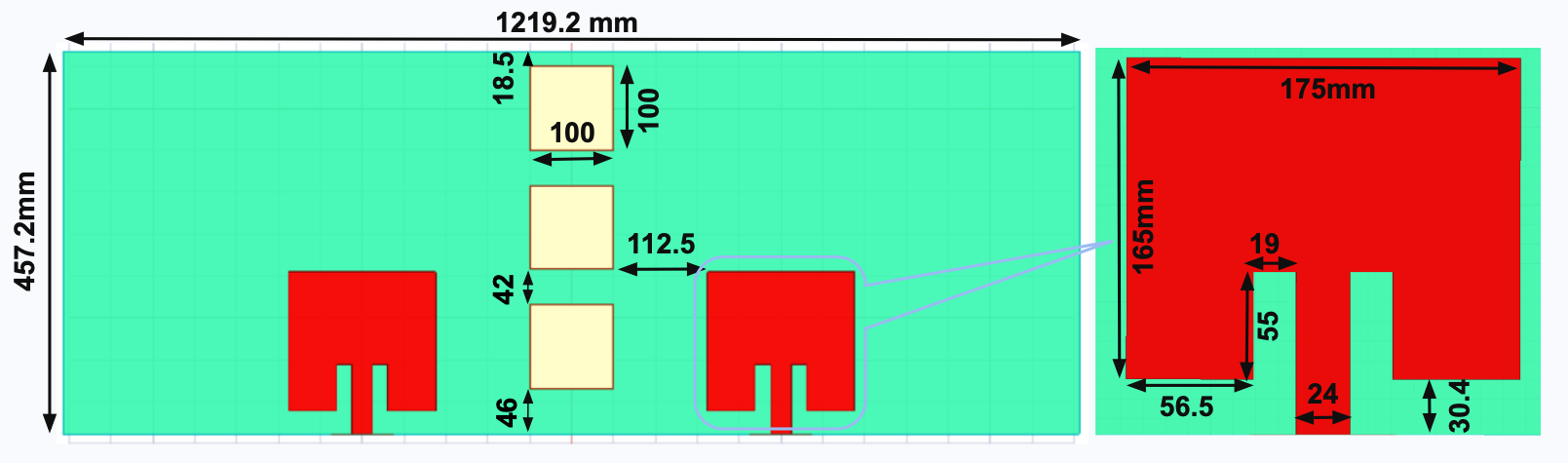
Design Framework and Criteria: The figure below illustrates the initial design of the full-duplex patch antenna element and its dimensions in the HFSS environment. The initial design includes symmetric patch antenna elements for Tx and Rx.
The EBG structure, represented by yellow squares, was strategically placed to enhance isolation. The substrate panel dimensions were set to 18′′ × 48′′ (457.2 mm × 1219.2 mm) to accommodate the patch elements and EBG structures.
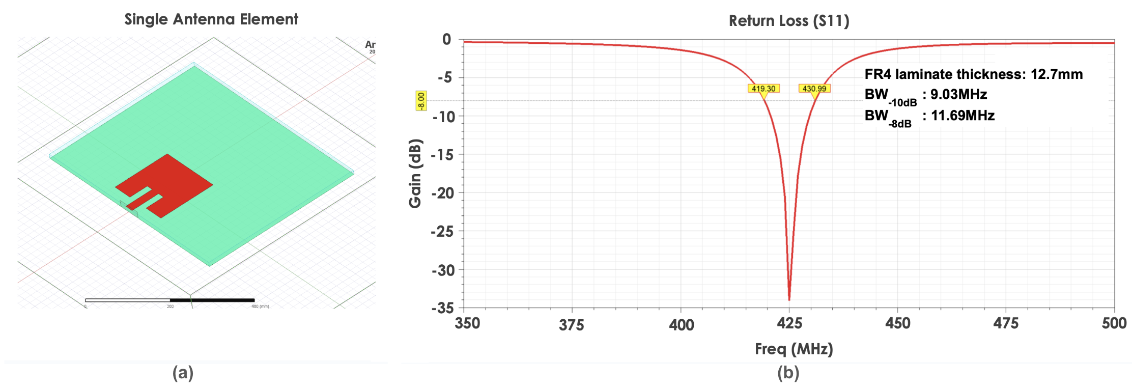
Left figure (a) below illustrates the simulated single antenna element in the HFSS environment, while right figure (b) presents the simulated return loss plot as a function of frequency. The target resonance frequency is 425 MHz. At a desired return loss of -10 dB or lower, the simulated bandwidth for the single antenna element is 9.03 MHz (420.92–429.95 MHz). For a return loss of -8 dB, the bandwidth increases to 11.69 MHz.
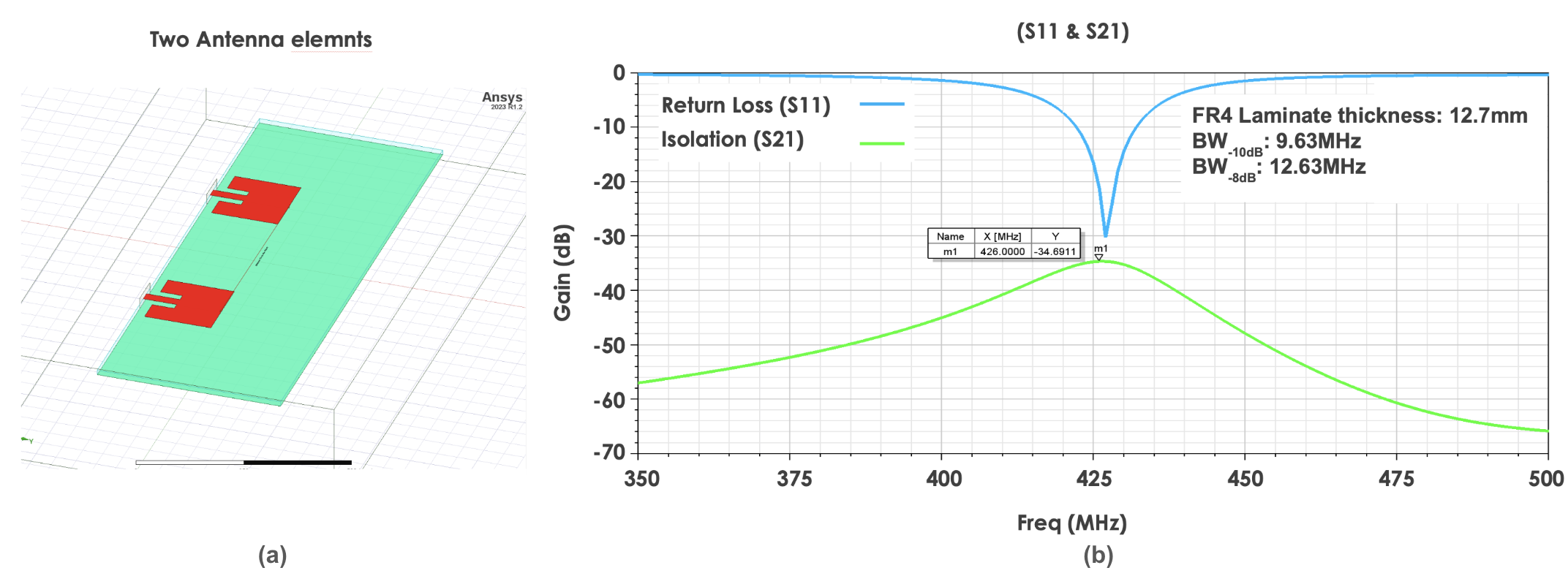
Left figure (a) below illustrates the simulated design of the FD antenna system after the addition of the second antenna element. right figure (b) presents the return loss and isolation after incorporating the second antenna element. The resonance frequency shifts to approximately 427 MHz, with a simulated bandwidth of 9.63 MHz at a return loss of -10 dB. The isolation between the two antenna elements is nearly -35 dB at the target frequency, without EBG integration.
Left figure (a) below shows the simulated FD antenna system in HFSS after adding EBGs. As observed in right figure (b), an isolation of nearly -64 dB is achieved by incorporating EBGs between the Tx and Rx antenna elements. The EBG structures have been refined to meet the target isolation of -50 dB or better. Post-fabrication testing will validate the performance against these simulation results in an indoor environment and an anechoic chamber.
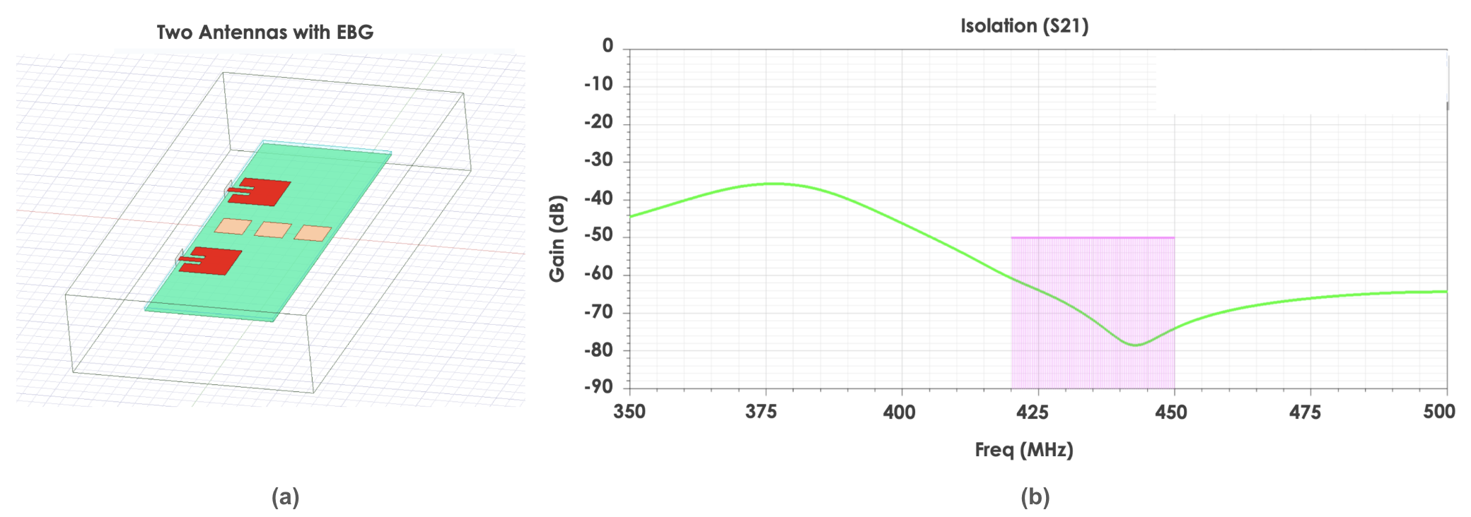
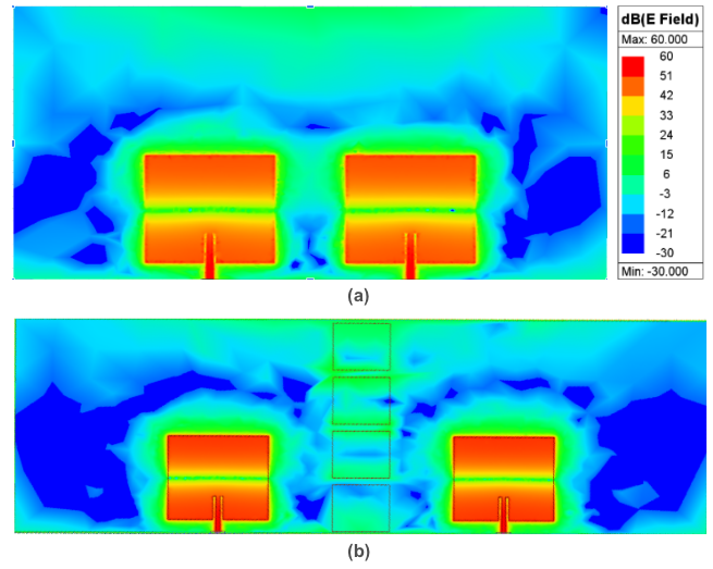
Figure (a) below shows a snapshot of the electric field distribution illustrating Tx-Rx mutual coupling without EBG. In figure (b), it is observed that the EBGs create a scattering path within the EBG structure, effectively reducing the mutual coupling.
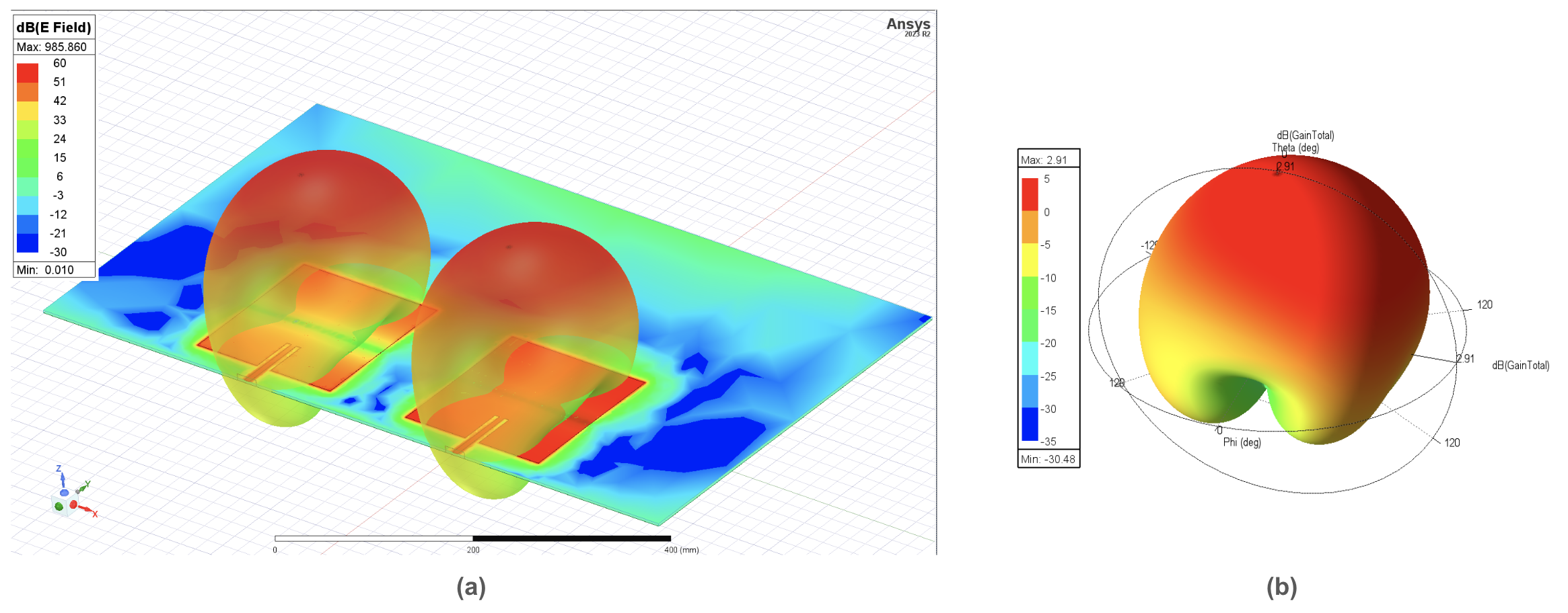
Radiation Pattern: Left figure below (a) illustrates a snapshot of the radiation pattern and coupling effect in an FD communication. Right figure (b) shows the simulated 3D radiation pattern of the unit antenna.
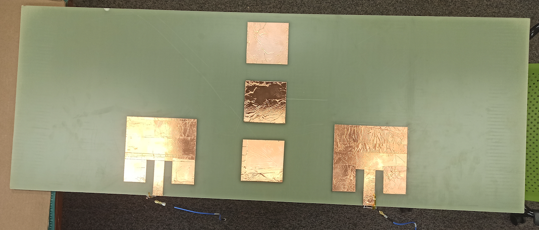
Fabrication methods: The prototype was fabricated manually by applying copper tape to unclad 18” x 48” x 0.5” FR4 substrate. This involved taping out the patch
antenna on the top side of the FR4 material, and covering the back side of the FR4 substrate with copper tape to form the ground plane. FR4 was chosen for
its affordability and suitability for operation in the VHF band. (The density and cost of FR4 was not ideal though: the antenna board weighed in at over 13.5 Kg
and cost over $400. 1 inch thickness FR4 would have had better electrical properties, but was rejected as impractically heavy and expensive.) Conductive-adhesive
copper tape was selected for its ease of application and conductivity, making it ideal for rapid prototyping.
Challenges in transitioning from design to fabrication:
One significant challenge is the manual precision required for taping out the patch antenna and ground plane with copper tape. Even minor misalignments of a few millimeters
can significantly impact performance, affecting resonant frequency, return loss (S11), and isolation (S21). Achieving precise alignment during fabrication is critical for
ensuring the antenna meets its design specifications. Figure below shows the initial fabrication of the antenna.